Defects in materials, such as atomic vacancies, doping, substitutions, and their combinations, can be beneficial in many cases. The Transforming Material Defect Creation and Application via AI-Driven Computation and Experiment cluster aims to develop an AI-driven approach to enable defect-by-design, and apply the AI framework to study quantum defects in two materials: silicon and hexagonal boron nitride (hBN). The team envisions an AI framework that can deepen our understanding of material atomic structures, thermodynamics, defect formation and evolution, as well as their relation to the electronic, optical, and spin properties.
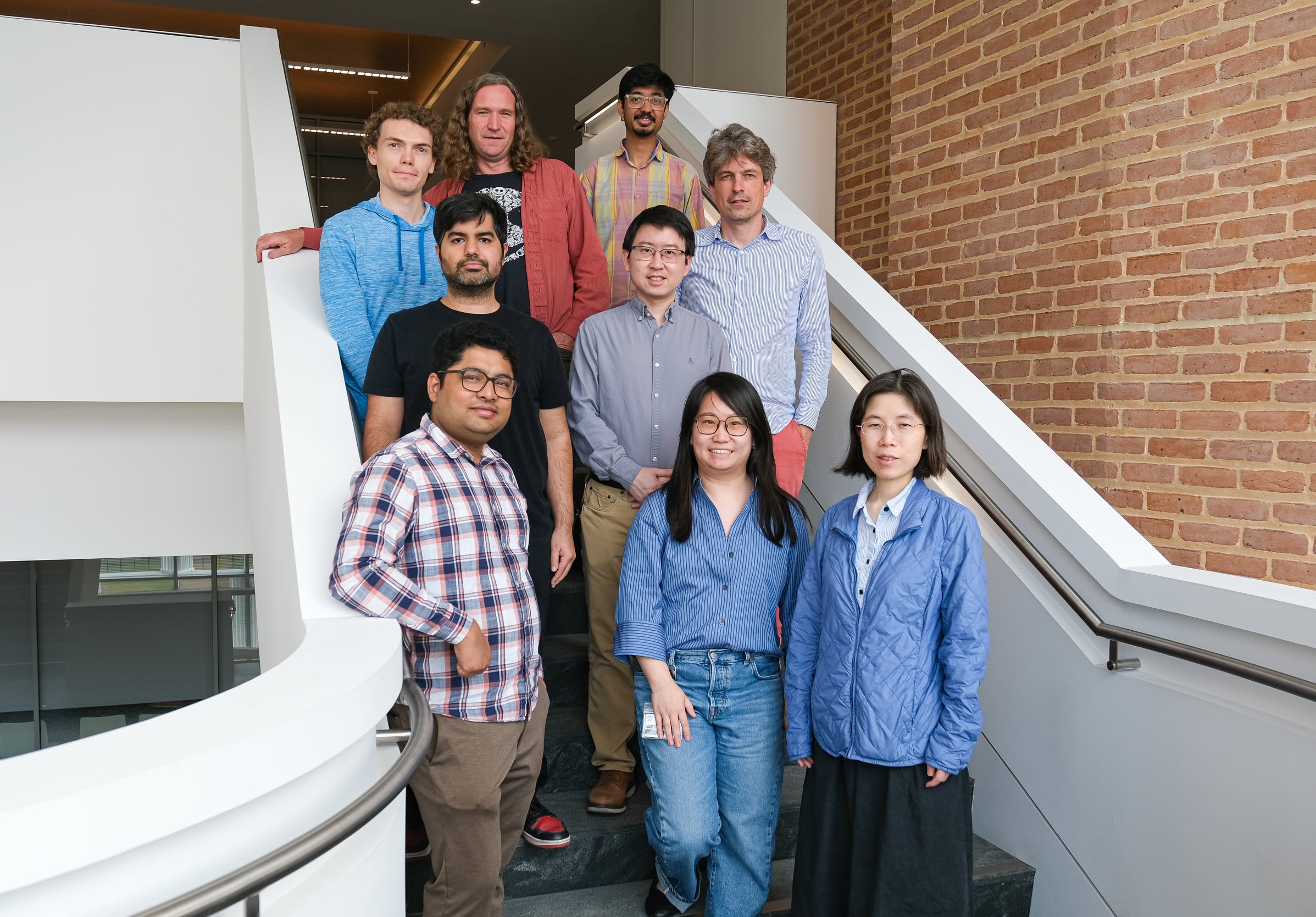
Cluster Members
- PI: Shengxi Huang (ECE)
- Co-Is: Geoffroy Hautier (MSNE), Songtao Chen (ECE & Physics), Christopher Jermaine (CS)
- Associates: Anastasios Kyrillidis (CS)
-
Research Vision
-
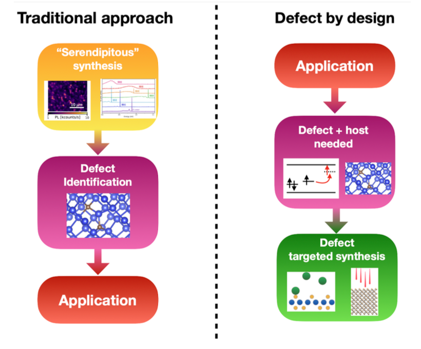
Defects in materials, such as atomic vacancies, doping, substitutions, and their combinations, can be beneficial in many cases. A famous example is doping in silicon that enables the entire semiconductor industry. Another recent example is the nitrogen-vacancy (NV) center in diamond that are key to quantum communication and sensing. Therefore, to design, manufacture, and understand defects in materials is critical. The traditional approach to study defects is based on serendipitous synthesis: a defect is randomly synthesized in the host material, then scientists study the defect experimentally and understand its properties, based on which applications are developed. However, this approach is uncontrollable and inefficient. These issues can be solved by a new approach, defect-by-design: first, an application is conceived, which places requirements for defect properties, based on which the specific defect is designed and the corresponding synthesis is implemented. However, to enable the new defect-by-design approach, significant challenges exist, including the huge design space (types of defects and host materials), lack of existing defect data both from experiments and first-principles calculations, and slow experimental process (synthesis, characterization, and tuning of synthesis recipe). In this project, we aim to develop an AI-driven approach to enable defect-by-design, and apply the AI framework to study quantum defects in two materials, silicon and hexagonal boron nitride (hBN).
Our long-term vision is to develop an ”AlphaFold” for materials: i) Given a host material, the AI framework will give a phase diagram of its defects (i.e., all the possible, stable defects). ii) Given a specific application, the AI framework will design the target defect. iii) Given a designer defect, the automatic experiment setup can synthesize the defect efficiently and accurately. Our ”AlphaFold” for materials will deepen our understanding of material atomic structures, thermodynamics, defect formation and evolution, as well as their relation to the electronic, optical, and spin properties. It will greatly accelerate the development of high-performance materials for various technologies and applications, including semiconductor chips that can support powerful large-language models, secure quantum communication networks that cannot be eavesdropped, and quantum sensors that have extreme sensitivity and precision down to the single-molecule level.